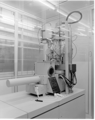
An electron beam pattern generator
Electron beam lithography is a process that can be used to write fine patterns with an electron beam. An electron beam can be generated by extracting electrons from a sharp needle with an electric field. If the electrons are then accelerated towards a metal plate with a small hole in it, a narrow beam of electrons emerges from this hole. The electrons are typically accelerated through a potential of several kilovolts and are traveling at a good fraction of the speed of light. An electron beam can be deflected by electric and magnetic field which makes it possible to write with the beam. Such electron beams are used in televisions and computer monitors. It is possible to focus an electron beam to have a very small diameter of about 1 nanometer. Such narrowly focused beams are used in scanning electron microscopes, transmission electron microscopes, and electron-beam pattern generators. Typically in an electron-beam pattern generator, the electron beam writes a pattern in a thin organic film that is coated over a wafer. Usually the wafer is a single crystal of silicon that is about 0.5 mm thick and 10 - 30 cm in diameter. The thin (~100 nm) organic film contains long molecules that wrap around each other like cooked spagetti. The energetic electrons in the electron beam cut these molecules up into small pieces. The film is then dipped in developer which disolves the short pieces but leaves the long unexposed sections unaffected. A pattern is thereby defined in the resist. The pattern can be transfered to the substrate by putting the wafer in a gas or liquid that dissolves the substrate material. Patterns with features of a few tens of nanometers can be made this way.
An electron beam pattern generator